This week, I started working on the laser schematic. There are many different types of laser drivers and multiple approach strategies for building such a project. This page is more dedicated to narrowing down the design approach than the schematic design itself.
So far, we have only narrowed the selection for the laser diode. Next, we need to decide which driver topology to use. When it comes to our application, we have two options, Buck, and Boost. Generally, Buck drivers, also known as step-down converters, are more energy efficient than their counterparts. Laser diodes are rather inefficient at converting electricity to visible light. Roughly half of the power supplied to the diodes turns into heat. That’s why it’s important to minimize the heating of other components as much as possible. Since our diode has 4 strings (channels) of 6 diodes each, to power the laser, we need a chip with 4 buck driver outputs.

Such a chip is the LM3464 from Texas Instruments. As seen in the figure above, the IC uses 4 MOSFETs to set the current to the diodes. For this configuration to be efficient, the voltage source must be close to the driving voltage of the diodes. Otherwise, the MOSFETs must dissipate excessive amounts of power, making the Buck driver inefficient. This becomes a problem since the voltage source powering the laser will be one 7S or two 4S LiPo batteries in series. Since batteries discharge over time, this gives us a possible swing of 8V. When driving the laser with 3.5A at 8V drop across the transistors, we get a total of 28W of power being dissipated by the MOSFETs.
However, there is a possibility that the driving mechanism is based on the PWM control, which would make it a bit more suitable. I have scheduled a meeting with professor Zahlava at CTU to discuss this matter further.

The other option is the Buck driver and after analyzing commercial PCBs featuring our diode, it seems that this type of driver is preferred. After a few hours of looking at Mouser, I have settled on the LT3756 LED controller from Analog Devices. The driver has a maximum input voltage of 100V; however, our diode will be running up to 103V. This is quite unfortunate, as the tiny difference may destabilize the phase integrity of the output signal. There is a simple workaround by choosing the resistor divider values with this difference in mind.

The last chip I was looking at is a MAX25600 Synchronous 4-switch LED Driver from Maxim Integrated. Synchronous drivers feature increased power efficiency; however, this comes at the cost of increased design complexity. Since we will be integrating the driver onto the laser interface module, this approach may become very hard to integrate. This week, I will talk to the professor regarding this issue.
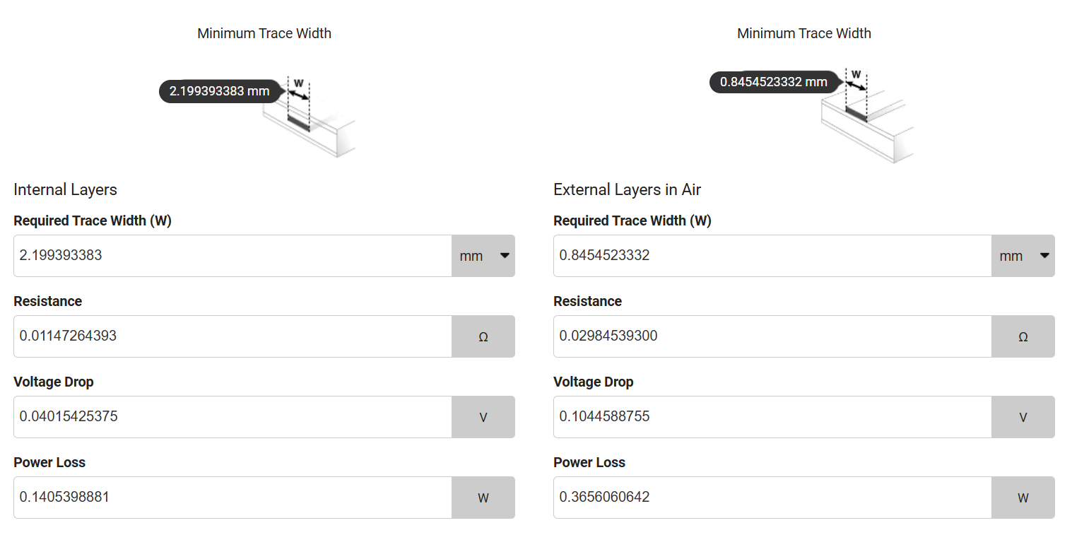
Another problem might arise from the thermal heating of the PCB. Since we are passing over 3A of current through the traces, we need to estimate what is the minimal viable track width. Due to space constraints, we can not afford more than 4mm thickness. After considering 2Oz copper plating, the required track is roughly 0.8mm. This falls well within our limit and thus the PCB can handle the high current.
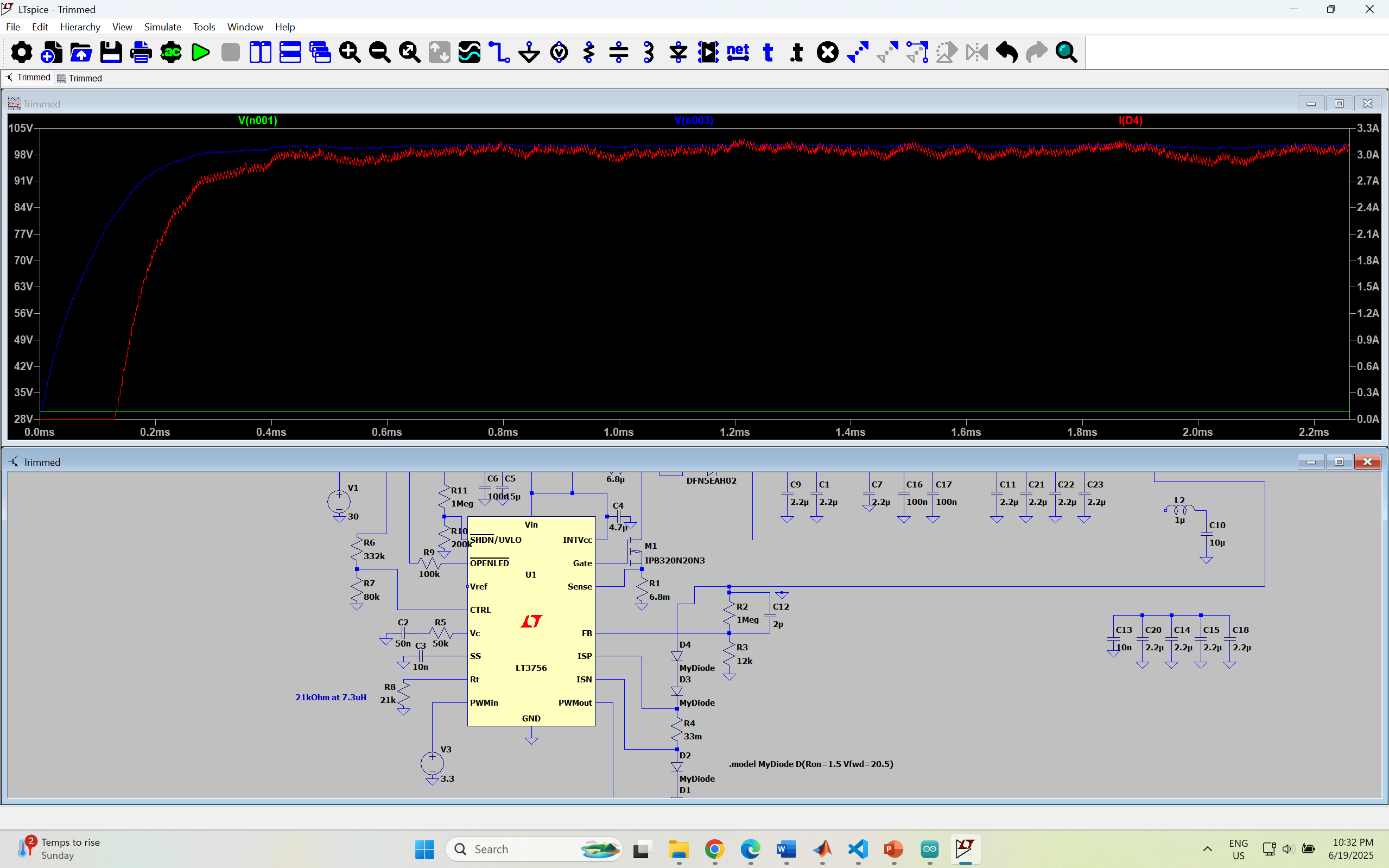
As mentioned earlier, this week's goal was to set up a simple simulation in LTspice. As I have never worked with this software before, I battled quite a steep learning curve. Nevertheless, simulating the circuit was a critical part of the entire design. To learn how to import the models, as seen on the screen, please refer to my Final Project blog.
Main design consideration was the current flowing through the diodes. In the simulation, the current ripple is around 300mA. It is important to note that this value is likely overestimated, as I designed the laser diode model with higher current power requirements than the real-world model.
The compensation network needs to be tuned to lower the ripple current. This is not a trivial task, however, and I aim to find the optimal values later using a mathematical model of the circuit. So far, the values have been chosen as a 70kOhm resistor and a 50nF capacitor. This changes the system’s dynamics, thus lowering the oscillations.
Furthermore, the value of 200mA is quite good, considering the 300W output of the regulator. Other important parameters include the current sensing resistors and the output voltage feedback network. Values for these components have been taken from the datasheet.
