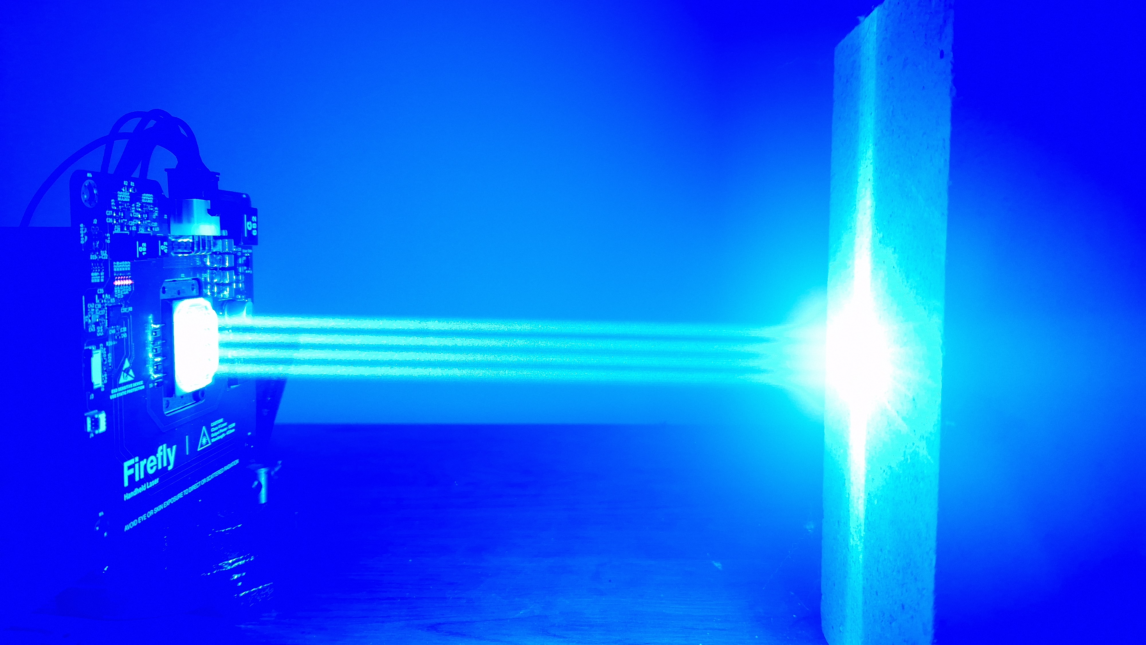
This project aims to build one of the most powerful handheld lasers in the world. While the legal limit for laser pointers sold in the EU is 1 milliwatt (mW), the laser I’m designing will exceed this limit by over 125,000 times. Although I originally aimed to break the world record for the strongest continuous-wave handheld laser, I was narrowly beaten by YouTuber and laser hobbyist Drake Anthony just three weeks before my design was ready. Despite this, I remained committed to improving the design and manufacturing a custom printed circuit board (PCB) to push the boundaries of what’s possible.
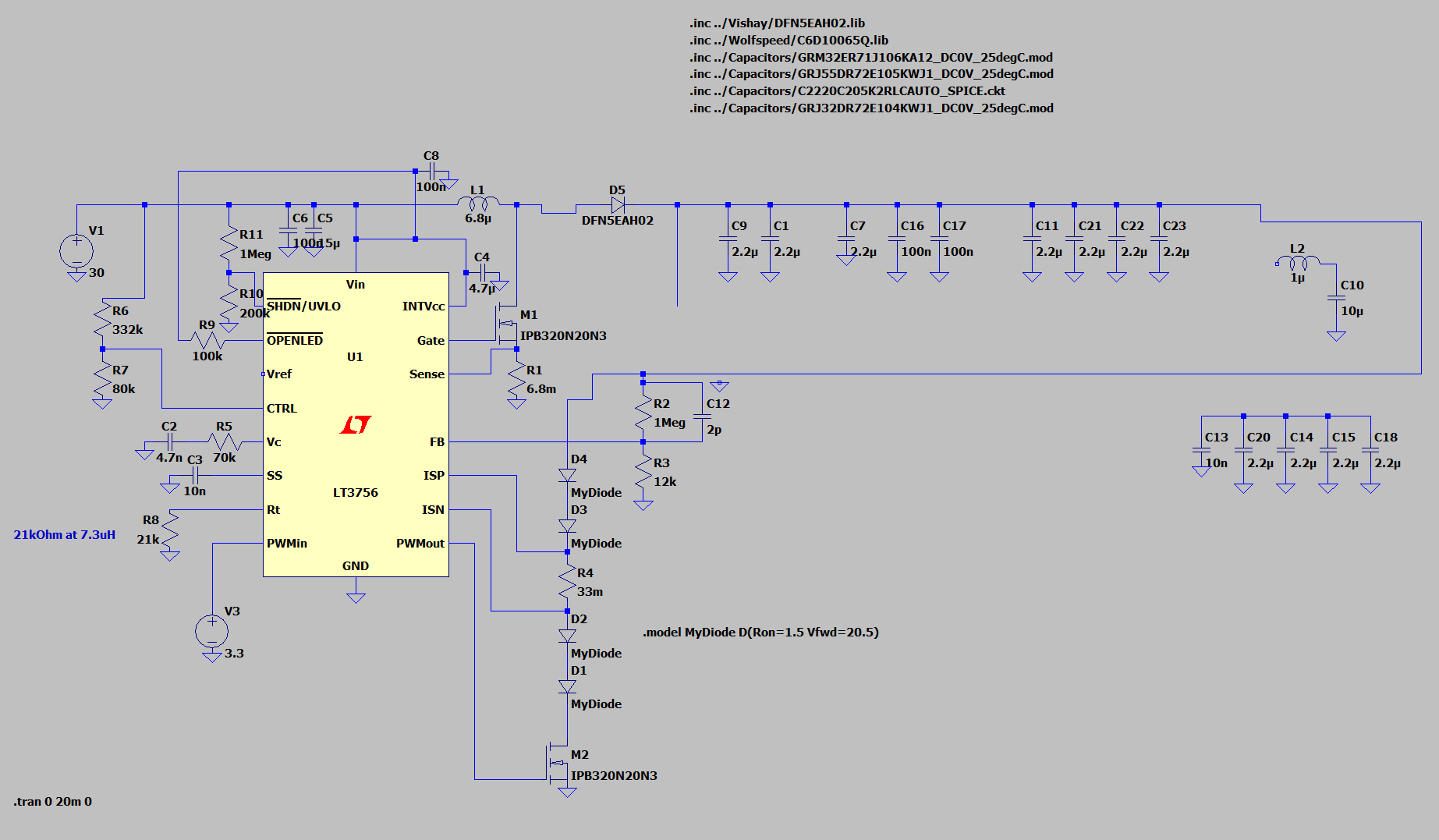
The first step in the design process was creating and simulating the circuit using LTspice. As I had limited experience with the software, I faced a steep learning curve, especially when it came to importing custom SPICE models—a critical step for accurate simulation. To organize my work, I began by creating a dedicated directory within the project folder, which made navigation within the component selector more efficient.
LTspice supports various SPICE file formats, such as .lib, .ckt, and .mod. Some manufacturers also provide an LTspice-specific symbol file, which, if placed in the same directory, is automatically recognized. To include custom models in a simulation, I used the .inc directive followed by the relative path to the model file—for instance, .inc ../Capacitors/GRM32ER71J106KA12_DC0V_25degC.mod. This directive is added using the SPICE directive tool, found either in the toolbar or by pressing the period (.) key.
Once the file is included, I applied the model to a component by control-right-clicking on it and entering the model name exactly as written in the header of the SPICE file. If no existing symbol matched, I created a new one by opening the file in LTspice, right-clicking the .model line, and selecting "Create Symbol." Finally, I ensured the component’s value field matched the model name.

With the models imported, I simulated key aspects of the circuit, including the feedback network, power consumption, compensation network, and feed-forward capacitor behavior. The schematic in LTspice reflects the final component values used.
During simulation, I found that introducing realistic equivalent series resistance (ESR) for output capacitors caused instability in the constant-current loop. To resolve this, I tuned the compensation network, and found that a 50 kΩ resistor and a 50 nF capacitor provided optimal stability. Although I calculated the phase and gain margins, the resulting plots weren’t directly helpful in identifying pole placements.
The output voltage feedback network also presented challenges. I calculated the resistor values using datasheet equations, but the circuit exhibited oscillations. To suppress this, I added a 2 pF capacitor across the 1 MΩ resistor in the divider, which acted as a low-pass filter, allowing fast transitions through while the resistor’s inductance caught up.

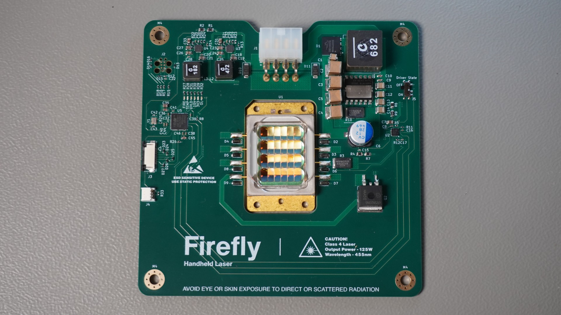
The complete schematic consists of three main sections: the laser driver, voltage regulation, and the microcontroller unit (MCU). I chose the LM3756 as the constant-current driver, mainly because a reliable SPICE model was available. At the time, no ICs capable of operating above 100 V were listed on Mouser. The laser diode array requires up to 105 V, which exceeded the chip’s capabilities. To work around this, I connected the sense resistor (between the ISP and ISN pins) midway through the diode array. This trick ensured the IC only sensed half the total voltage, allowing the rest of the circuit to function unchanged.

I selected a switching frequency of 1 MHz to minimize the size of passive components. However, this choice introduced another challenge: high-current MOSFETs suitable for the power level tend to have high gate capacitances and Rds(on) values. Interestingly, the majority of power losses at this frequency come not from conduction, but from switching. This made gallium nitride (GaN) FETs an attractive alternative, due to their low gate charge and low on-resistance, making them ideal for high-frequency applications.
Still, GaN transistors posed their own challenges. Most have a maximum gate-source voltage (Vgs) of 6–7 V, while the LM3756 drives the gate up to 7.3 V. Exceeding this voltage risks damaging the transistors, but the chip also has a minimum Vcc of 6 V, leaving an uncomfortably narrow safety margin. A mere 0.5 V difference in either direction could cause failure. To manage this, I sourced a GaN FET with a higher gate threshold voltage, at the expense of increased gate capacitance and on-resistance. Even with this tradeoff, the selected FETs still outperformed standard MOSFETs rated for similar loads.
The final major design hurdle was selecting suitable output capacitors for the constant-current stage. I needed at least 7 µF of capacitance rated for 120 VDC with low ESR to avoid destabilizing the feedback loop. Additionally, performance at 1 MHz was crucial. Electrolytic capacitors were eliminated due to their poor high-frequency response. This left three viable types: MLCCs, film, and polymer capacitors. Film capacitors were ruled out for being too bulky to fit in the handheld design. Polymer capacitors, while having higher ESR, were acceptable in bulk capacitance roles. I included 12 µF of polymer capacitors to help handle transient high loads. MLCCs offered excellent high-frequency performance and low ESR, but suffered from severe voltage derating. For example, a 250 V-rated capacitor could lose 60% of its capacitance at just 102 V. To compensate, I used twelve MLCCs arranged in four rows with three capacitors stacked vertically in each row—an expensive solution in terms of both space and cost.

The MCU section serves as a safety mechanism. It verifies the power-good signals from the regulators and waits for a user command before enabling the laser.
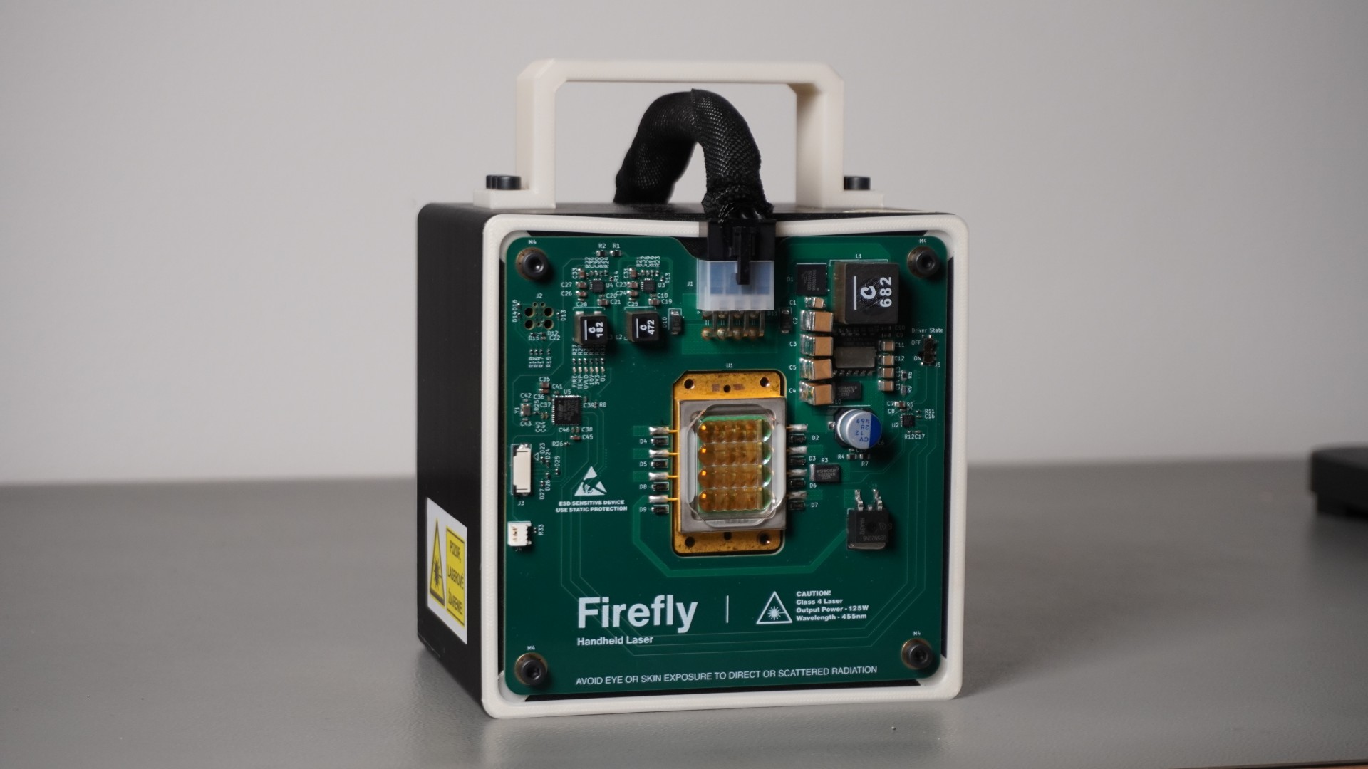
For now, the laser’s enclosure is temporary and designed to facilitate testing. It will eventually be replaced by a custom aluminum chassis. Thermal management is critical—temperatures above 70 °C can damage the laser diodes. For initial tests, the diode is mounted to a massive 11x10 cm aluminum cylinder, which acts as a thermal buffer, allowing the laser to run for a few minutes. However, this solution is impractical due to its weight. A promising future upgrade is a 3D-printed copper heatsink with active cooling, which could significantly reduce size and weight.
The enclosure comprises six main components: the PCB, the main housing containing the heatsink, an end cap to retain the heatsink, a protective rim, the heatsink itself, and a handle for safe carrying. All components were designed in Fusion 360.
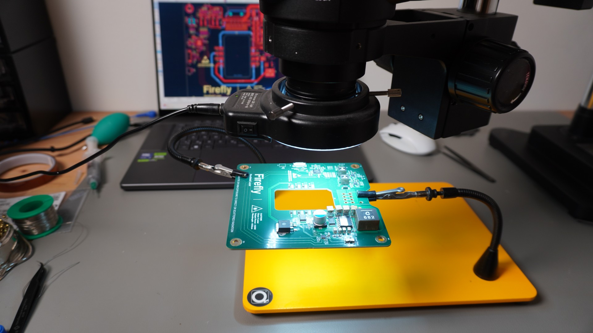
Assembly of the laser was done entirely by hand. Due to the small component sizes—most are 0402 packages—it took several hours to complete. Custom Molex connectors were also crimped to handle the high currents involved.
A second PCB functions as an auxiliary unit, supplying power and incorporating basic safety features to prevent accidental activation. Two XT60 connectors link two 4S LiPo batteries in series to provide approximately 30 V. A ribbon FFC cable handles shielded SPI communication with the MCU and transmits the enable signal to the laser driver. In the future, this board will be replaced by a dedicated MCU that will serve as the primary control unit.


A few issues arose during the bring-up of the device. In the schematic, there is a flipped ISP and ISN pair from the sense resistor. Furthermore, the footprint for the GaN driver had to be slightly altered. After these changes, however, the laser became fully operational. Additionally, a small heatsink needed to be installed on the GaN FET, as it was heating more than expected. This may be a byproduct of the switching frequency having been set to 500 kHz instead of the planned 1 MHz for testing.
Below are photos of the completed assembly.