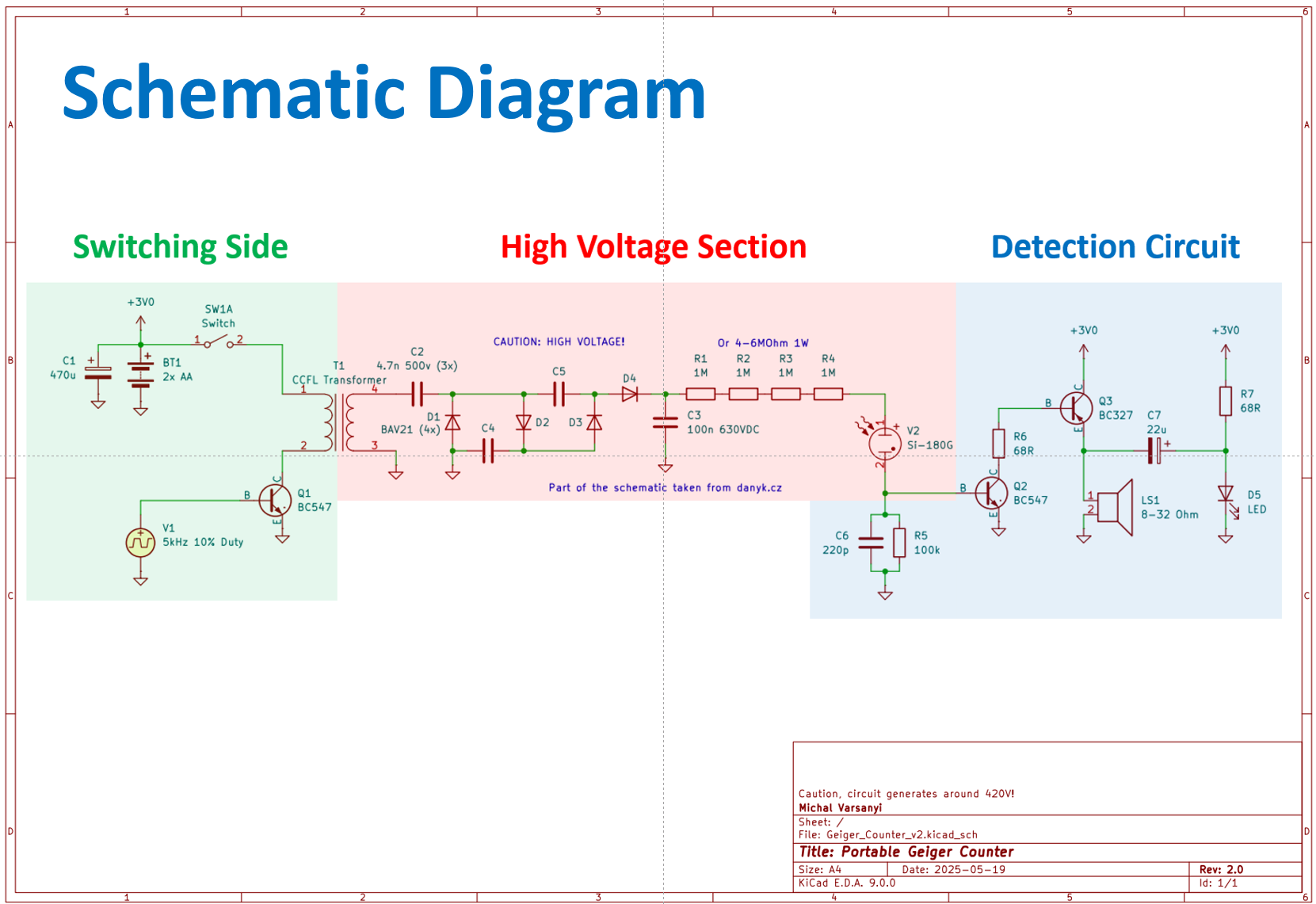
This week, we will be using interface sensors. Luckily, there has been a very special one lying on my shelf for quite some time. Six years ago, I bought an old Soviet Geiger tube from Moscow. It is the SI-180G (СИ-180Г) manufactured by ZELTA in the USSR. It is one of the best tubes for measuring background radiation. Apart from that, it has really poor performance in measuring direct sources. That’s why this week; we will be building a Geiger counter from scratch.
DISCLAIMER: Due to its difficulty, this is still an ongoing project. I will post the results by the end of the semester.
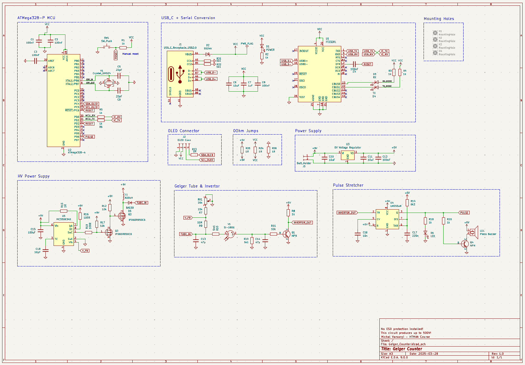
The design is based on the Do-It-Yourself (DIY) Geiger Counter from MIT. For further details about the circuit, please refer to their Instructions. I have modified the scheme to work with parts in stock at a popular electronics store in Prague. I have decided to go SDM (components soldered on top of the board) to improve the design of the boost converter. This goes without saying, manufacturing one-sided PCBs on a milling machine is signal integrity and RF mayhem. Consequently, this week’s goal is just to make a proof of concept and then order a proper board.
I have tried to minimize the number of blue wire (taking a small cable and connecting it manually) interconnections, and at the end of the day, I have used just one. I did not pay too much attention to the regulator design, as it will likely have negligible effect compared to the missing ground planes.

The plan was to manufacture the PCB on the Carvera Air CNC Machine. As it turns out, making such a complicated PCB on a CNC router is rather difficult. I have spent multiple days trying to manufacture the board. In fact, it would be done quicker, if I’d order the PCBs from China directly. However, a huge thanks goes to Krištof Pučejdl for his time, weekend and effort in helping me with the PCB. Without his help, I would not be able to make the PCB as quickly as I did.
The Carvera must have a minimum of 0.2mm of clearance between tracks. Since I have integrated a USB to UART converter using USB-C, I could just barely get away with 0.2mm trace widths and clearances. This will later prove to be the bottleneck of the entire design. We have exported the .kicad_pcb files into Fusion360, where we’ve set the CNC path and tooling dimensions. We have decided to route the paths first and then drill the holes.
After the first PCB was manufactured, we applied a red solder mask, which was later cured under UV light. The board was covered with resin multiple times. The problem began when we started routing all the covered pads. Carvera uses a special spring-loaded tool, which gets pressed against the board and routes only the resin layer. Routing through-hole contacts, the machine first started inside of the hole and then moved out to remove the solder mask. Unfortunately, the tip of the spring-loaded tool could not jump from the hole and routed the entire pad out. Furthermore, some smaller tracks were ripped off as well. I have observed this happening only with the 0.2mm tracks and an unconnected pads of the integrated circuits. Since they were not connected, they did not hold as the router passed over them.

The next day, I made a new PCB without the mask. In this case, to increase the precision, we have set the calibration points to roughly for 4x6 marks for width x height. This, however, did not help at all and some of the 0.2mm traces got destroyed again. Moving on, I have started soldering the board without the USB-MCU interface. Unfortunately, I forgot to buy the boost IC, thus I could not get the project finished in time.


I have decided to make a simpler version of the circuit on a prefboard. The boost converter is switched using a Raspberry Pi Pico. The following code can be seen below. It is important to note, that it only works with the arduino-pico board repository, which includes the analogWriteFreq command.
        const int PWM_PIN = 16;

        void setup() {
        analogWriteFreq(5000);  // Set PWM frequency to 50kHz
        analogWrite(PWM_PIN, map(10, 0, 100, 0, 255));  // 50% duty cycle on 8-bit scale (0–255)

        pinMode(LED_BUILTIN, OUTPUT);
        }

        void loop() {
        // PWM continues automatically

        digitalWrite(LED_BUILTIN, HIGH);  // turn the LED on (HIGH is the voltage level)
        delay(1000);                      // wait for a second
        digitalWrite(LED_BUILTIN, LOW);   // turn the LED off by making the voltage LOW
        delay(1000);
        }